Cadence Enables Next-Gen AI and HPC Systems with Industry’s Fastest HBM4 12.8Gb IP Memory System Solution
With 20% greater power efficiency/bit and 50% better area efficiency while doubling number of IOs for higher bandwidth
This is a Press Release edited by StorageNewsletter.com on April 21, 2025 at 2:00 pmCadence Design Systems, Inc. announced the industry’s fastest HBM4 12.8Gb memory IP solution, which meets the increasingly higher memory bandwidth needs of SoCs targeted for the next-gen of AI training and HPC hardware systems.
![]()
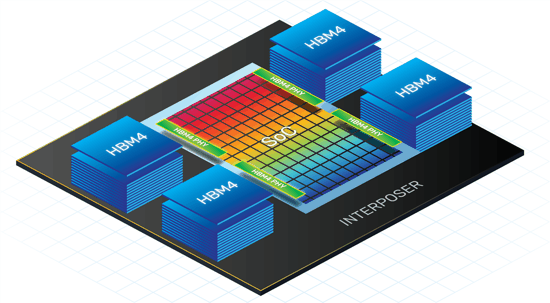
The Cadence HBM4 solution is compatible with the JEDEC specification JESD270-4 and doubles the memory bandwidth compared to the previous-gen of HBM3E IP products. Available now for customer engagements, the company’s HBM4 PHY and controller IP boast an industry-leading performance of 12.8Gb, with 20% greater power efficiency per bit and 50% better area efficiency while doubling the number of IOs for higher bandwidth.
The firm’s HBM4 IP offers a PHY and a high-performance controller as a complete memory subsystem solution. The HBM4 PHY will be available as a drop-in hardened macro in the TSMC N3 and N2 technology nodes, while the HBM4 controller will be provided as a soft RTL macro. The best-in-class 12.8Gb data rate exceeds the available HBM4 DRAM device speeds by 60% – giving designers ample system margin, enabling support for potential speed improvements, and future-proofing their SoC products. The high-performance, low-latency architecture includes RAS and BIST features for fine-tuning memory subsystem performance in the field for optimal data center operations. The standard HBM4 IP offering includes support for all flavors of interposer design implementation options and lab software for rapid memory subsystem bring-up of customer SoCs.
“The proliferation of generative and agentic AI applications and the resulting increase in AI workloads demand higher memory bandwidth for greater AI hardware system efficiency without further draining power. Cadence’s HBM4 solution addresses this insatiable need for memory bandwidth by providing the highest performance available at 12.8Gbps while maintaining area and power efficiency – key concerns for AI factories,” said Boyd Phelps, SVP and GM, silicon solutions group, Cadence.
Cadence’s HBM4 solution includes a comprehensive set of deliverables for faster integration of the IP to SoC design and post-silicon bring up. The deliverables include a reference interposer design validated at 12.8Gb on a full-featured test chip consisting of an HBM4 controller, PHY, interposer, and HBM4 DRAM device. LabStation software with extensive features and test suites for rapid SoC post-silicon lab bring-up is provided for faster time to market.
Cadence’s HBM4 PHY and controller have been verified with the company’s Verification IP (VIP) for HBM4 to provide rapid IP and SoC verification closure. Cadence VIP for HBM4 includes a complete solution from IP to system-level verification with DFI VIP, HBM4 memory model, and System Performance Analyzer.
Resource:
Blog: HBM4 Boosts Memory Performance for AI Training


 Subscribe to our free daily newsletter

