Argonne National Laboratory to Lead Two Microelectronics Research Projects Under U.S. Department of Energy Initiative
Ultra dense memory: atom scale material dynamics and systems consequence, and BIA: Co-design methodology to transform materials and computer architecture research for energy efficiency
This is a Press Release edited by StorageNewsletter.com on January 13, 2025 at 2:02 pmThe U.S. Department of Energy’s (DOE) Argonne National Laboratory is managing 2 microelectronics studies that will support multidisciplinary codesign of hardware and software and enable processing of vast quantities of data at unprecedented speeds.
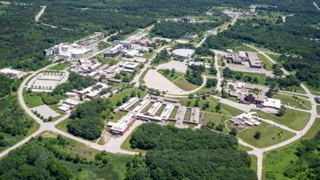
Argonne National Laboratory
(Image by Argonne National Laboratory)
Argonne is a premier research institution in microelectronics, the tiny devices that power and control computers, smartphones, electric vehicles and other information processing equipment. It also leads the projects as part of DOE’s Microelectronics Science Research Centers.
In December 2024, DOE’s Office of Science announced $160 million in funding to establish the research centers, which are being implemented through the historic CHIPS and Science Act of 2022. The centers will focus on microelectronics technologies for computing, communication, sensing and power. Researchers in the microelectronics field seek transformative advances in energy efficiency and/or resilience in extreme environments.
One of the Argonne projects, Ultra Dense Memory: Atom Scale Material Dynamics and Systems Consequences will be led by Supratik Guha, senior adviser, Argonne’s Physical Sciences and Engineering directorate. The University of Chicago, Purdue University, the Georgia Institute of Technology and Chicago State University are academic partners, and IBM Corp. and Micron Technology, Inc. are industrial collaborators.
The project will focus on future-gen of extreme-scale memories — architectures and technologies designed to handle massive amounts of data at exceptionally high speeds, needed for tomorrow’s high-performance computers and sensors — and their synthesis for on-chip and off-chip applications. This project is part of DOE’s Extreme Lithography and Materials Innovation Center.
The other project, BIA: A Co-Design Methodology to Transform Materials and Computer Architecture Research for Energy Efficiency, will be led by Valerie Taylor, Argonne Distinguished Fellow, mathematics and computer science division director. Lab and university partners are Fermi National Accelerator Laboratory, The University of Chicago, Northwestern University and Rice University. Named for the Olympian goddess of force and energy, the BIA project includes an industry advisory board with representatives from AMD (Advanced Micro Devices, Inc.), Enosemi, Lam Research Corp., Northrop Grumman Corp. and Nvidia Corp.
The goal of BIA is to develop a codesign methodology for microelectronics that considers the relationships between vertically stacked, integrated electronics. Codesign for microelectronics requires a multidisciplinary team consisting of researchers in materials design, devices, computer systems and applications such as high energy physics, working together to address the unique application needs. BIA is part of the Microelectronics Energy Efficiency Research Center for Advanced Technologies.


 Subscribe to our free daily newsletter

