Floadia Completes eFlash IP Qualification on TSMC 130BCD Plus Process and Achieves Highest Data Retention for 10 Years at 200°C
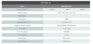
G1 is SONOS-type memory cell and it uses Fowler-Nordheim tunneling for program and erase operations.
This is a Press Release edited by StorageNewsletter.com on March 10, 2023 at 2:02 pmFloadia Corporation, a developer of embedded flash memory IP cores (eFlash IP) based in the Tokyo, Japan, suburb of Kodaira-shi, has completed qualification of its eFlash IP, G1, on the 130BCD Plus process of TSMC (Taiwan Semiconductor Manufacturing Company), the world’s largest semiconductor foundry headquartered in Taiwan.
![]()
G1 passed the qualification criteria of data retention for 10 years at 125°C after 10,000 program and erase operations. The same test was conducted at an even higher temperature of 200°C, and G1 achieves the world’s highest quality level of data retention for 10 years.
The BCD process is a process technology that enables the integration of 3 types of devices on a single chip: bipolar, CMOS, and DMOS. The BCD process technology gets more and more attention because it is indispensable for the realization of ‘smart power management IC.’ This type of IC integrates a power management IC, which handles high voltages and large currents, and an MCU (microcontroller) on a single chip. At the same time, demand for NVM (memory that retains data even when the power is turned off) on the BCD process is increasing to store programs and various parameters in the MCU.
The ‘hot electron injection floating gate’ MTP has been regarded as the most promising NVM for the BCD process because it requires almost no additional process steps. However, this type of MTP has the risk of poor data retention caused by stress-induced leakage current (SILC). Failure to read data correctly can lead to a major quality failure. Circuit design is usually adopted to reduce the risk, but, in the meantime, it increases the cost due to the large chip size.
The company’s G1 is a SONOS-type memory cell and it uses Fowler-Nordheim (FN) tunneling for program and erase operations.
This offers the following advantages:
1) low power consumption during rewrite,
2) small IP size,
3) high data retention because of no SILC phenomenon,
4) only 3 additional masks required, and
5) short test and bake times.
Moreover, the thermal budget of G1’s additional processes won’t affect the existing BCD devices. For this reason, the process design kit (PDK) provided by the foundry and the SPICE models (models describing the operation of transistors and passive devices) included in the PDK can be kept the same. As a result, chip companies can reuse all existing IP assets while adding G1, and thus reducing product development time.
With the completion of G1 qualification on the TSMC 130BCD Plus process, the company will continue to support G1-based products; G1 is suitable for wireless charger ICs, USB power supply ICs, motor driver ICs, and programmable mixed-signal ICs. Some automotive electronic control unit applications have adopted G1 to reduce PCB size by 60% and weight by 80% by one integrated chip which was previously composed of multiple discrete components.
“Our G1 was firstly used in several smartphone ICs shortly after the company was founded in 2011. Since then, G1 adoption has expanded to multiple foundries and IDMs, from consumer chips to automotive chips,” said Kosuke Okuyama, president. “We are pleased that G1’s qualification on the TSMC 130BCD Plus process will facilitate the integration of smart power management ICs, which has been expected for long.“


 Subscribe to our free daily newsletter

