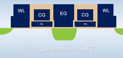
SST Qualified Embedded SuperFlash on 110nm Complementary Metal-Oxide-Semiconductor Process
ESF3 technology available to fabless and integrated device manufacturers
This is a Press Release edited by StorageNewsletter.com on February 24, 2017 at 2:55 pmMicrochip Technology Inc., a provider of micro-controller, mixed-signal, analog and Flash-IP solutions through its Silicon Storage Technology, Inc. (SST) subsidiary, announced qualification and availability of SST’s third-generation embedded SuperFlash (ESF3) non-volatile memory (NVM) on 110nm Complementary Metal-Oxide-Semiconductor (CMOS) platform.
SST’s embedded SuperFlash memory solution offers low power, reliability, data retention and endurance benefits to smart card, micro controller (MCU) and other flash-enabled specialized IC designers with a cost-effective, embedded flash solution. In smart card applications, the fast erase time and low power offers a low energy envelope that is critical for enabling low-power applications such as Near Field Communication (NFC) and dual-interface smart cards.
For the first time SST’s ESF3 technology is available to fabless and Integrated Device Manufacturers (IDMs) on a cost-effective 8-inch 110nm CMOS platform. This ESF3 platform is qualified for 300,000 erase and program cycles, making it suited for smart card and other high-endurance IC designs.
“The combination of low-power ESF3 technology on an advanced 110nm process node opens up exciting new product opportunities, especially for the secure smart card market,” said Vipin Tiwari, director of worldwide marketing and business development, SST. “Now customers who require low-power, high-endurance embedded Flash can keep production costs down by using this mainstream 8-inch CMOS platform.“


 Subscribe to our free daily newsletter

