Toshiba 32GB Embedded NAND Flash Memory Modules Up to 128GB
19nm process technology, Jedec e-MMC v5.0 compliant
This is a Press Release edited by StorageNewsletter.com on November 5, 2013 at 2:36 pmToshiba America Electronic Components (TAEC) announced its new embedded NAND flash memory modules.
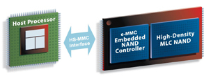
They integrate NAND chips fabricated with Toshiba’s 19nm second generation process technology and are compliant with the latest e-MMC (1) standard. Designed for application in a range of digital consumer products, the modules are targeted to smartphones, tablet PCs and digital video cameras.
Demand continues to grow for large density NAND flash memory chips that support high resolution video and deliver enhanced storage. This is particularly true in the area of embedded memories with a controller function, which minimize development requirements and ease integration into system designs.
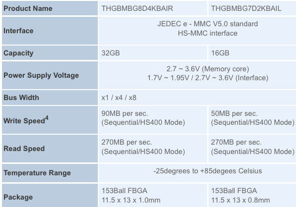
The new 32GB (2) embedded device integrates four 64Gb (equal to 8GB) NAND chips fabricated with Toshiba’s 19nm second generation process technology and a dedicated controller into a package measuring 11.5x13x1.0mm. It is compliant with JEDEC e-MMC Version 5.0, published by JEDEC in September, and achieves a high read/write performance by applying the new HS400 high speed interface standard.
The new line-up of single-package embedded NAND flash memories includes densities from 4GB to 128GB. Each device integrates a controller to manage basic control functions for NAND applications.

Key Features
- The JEDEC -MMC V5.0 compliant interface handles essential functions, including writing block management, error correction and driver software. It simplifies system development, allowing manufacturers to minimize development costs and speed up time to market for new and upgraded products.
- Embedded in a system, the 128GB module can record up to 2,222 hours of music at a 128Kbps bit rate, 16.6 hours of full spec high definition video and 38.4 hours of standard definition video3 The new products apply NAND flash memory chips fabricated with Toshiba’s leading-edge 19nm second generation process technology.
- The new products are sealed in a small FBGA package measuring 11.5x13mm, and have a signal layout compliant with the JEDEC e-MMC V5.0.
(1) e-MMC is a trademark and a product category for a class of embedded memory products built to the JEDEC e – MMC Standard specification.
(2) Product density is identified based on the density of memory chip(s) within the Product, not the amount of memory capacity available for data storage by the end user. Consumer-usable capacity will be less due to overhead data areas, formatting, bad blocks, and other constraints, and may also vary based on the host device and application. Maximum read and write speed may vary depending on the host device, read and write conditions, and file size.
(3) HD and SD are calculated at average bit rates of 17Mbps and 7Mbps, respectively.
(4) Read and write speed may vary depending on the read and write conditions, such as devices you use and file sizes you read and/or write.


 Subscribe to our free daily newsletter


