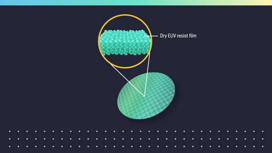
Lam Research EUV Dry Photoresist Technology Adopted by Leading Memory Manufacturer
Aether advanced patterning solutions enhance precision and cost efficiency to accelerate production of next-gen DRAM.
This is a Press Release edited by StorageNewsletter.com on February 4, 2025 at 2:00 pmLam Research Corp. announced that Aether its dry photoresist technology, has been selected by a leading memory manufacturer as production tool of record for the most advanced DRAM processes.
Aether dry photoresist technology extends resolution, productivity
and yield of Extreme Ultraviolet (EUV) lithography,
A breakthrough introduced by Lam in 2020, dry resist extends the resolution, productivity, and yield of Extreme Ultraviolet (EUV) lithography, a pivotal technology used in the production of next-gen semiconductor devices.
Lam’s dry resist approach overcomes the biggest challenges of transferring fine DRAM designs to a wafer.
“Lam’s dry resist approach overcomes the biggest challenges of transferring fine DRAM designs to a wafer, delivering low-defect, high fidelity precision, while also offering key advantages in cost and sustainability,” said Vahid Vahedi, chief technology and sustainability officer, Lam Research. “We are proud to collaborate with industry leaders to accelerate this DRAM patterning innovation into high-volume manufacturing.”
The memory manufacturer will employ the Aether tools in its most advanced DRAM nodes to form dry resist underlayers and films, and to use dry development processes. These processes overcome the traditional tradeoff between exposure dose and manufacturing defectivity to enable precise, low-defect patterning. This advancement drives down costs and enhances scanner productivity in the manufacturing of next-gen semiconductor devices.
Energy and compute intensive applications require continued scaling of memory capacity in an ever-smaller footprint to enable lower cost per bit of data. A key enabler of this scaling is industry-wide adoption of EUV lithography. The company’s dry photoresist technologies optimize the patterning process from resist application and stack deposition through final etching and cleaning, offering several advantages over conventional chemically amplified resist patterning.
Aether significantly enhances EUV sensitivity and the resolution of each wafer pass, enabling the most challenging patterns to better adhere to the wafer and improving performance and yield. In addition, it offers key sustainability benefits by consuming less energy and five to ten times less chemicals than traditional wet chemical resist processes.


 Subscribe to our free daily newsletter

