University of Pennsylvania: Breakthrough in Energy-Efficient Avalanche-Bbased Amorphization Could Change Storage
R&D on phase-change memory materials
This is a Press Release edited by StorageNewsletter.com on November 13, 2024 at 2:02 pm![]() By Ian Scheffler, senior science writer, Penn Engineering, School of Engineering and Applied Science, University of Pennsylvania
By Ian Scheffler, senior science writer, Penn Engineering, School of Engineering and Applied Science, University of Pennsylvania
The atoms of amorphous solids like glass have no ordered structure; they arrange themselves randomly, like scattered grains of sand on a beach. Normally, making materials amorphous – a process known as amorphization – requires considerable amounts of energy. The most common technique is the melt-quench process, which involves heating a material until it liquifies, then rapidly cooling it so the atoms don’t have time to order themselves in a crystal lattice.
Researchers at the University of Pennsylvania School of Engineering and Applied Science (Penn Engineering), the Indian Institute of Science (IISc) and the Massachusetts Institute of Technology (MIT) have developed a new method for amorphizing at least one material – wires made of indium selenide, or In2Se3 – that requires as little as one billion times less power density, a result described in a new paper in Nature. This advancement could unlock wider applications for phase-change memory (PCM) – a promising memory technology that could transform data storage in devices from cell phones to computers.
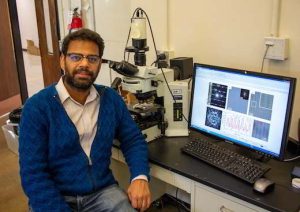
Ritesh Agarwal poses with some of equipment used in studying new process,
which dramatically lowers energy cost of amorphization,
bringing phase-change memory devices closer to commercial applicability.
Phase-Change Memory (PCM)
In PCM, information is stored by switching the material between amorphous and crystalline states, functioning like an on/off switch. However, large-scale commercialization has been limited by the high power needed to create these transformations.
“One of the reasons why PCM devices haven’t reached widespread use is due to the energy required,” says Ritesh Agarwal, Srinivasa Ramanujan distinguished scholar and professor, Materials Science and Engineering (MSE), Penn Engineering and one of paper’s senior authors.
For more than a decade, Agarwal’s group has studied alternatives to the melt-quench process, following their 2012 discovery that electrical pulses can amorphize alloys of germanium, antimony and tellurium without needing to melt the material.
Several years ago, as part of those efforts, one of the new paper’s 1st authors, Gaurav Modi, then a doctoral student in MSE, Penn Engineering, began experimenting with In2Se3, a semiconductor with several unusual properties: it is ferroelectric, meaning it can spontaneously polarize, and piezoelectric, meaning that mechanical stress causes it to generate an electric charge and, conversely, that an electric charge deforms the material.
New approach to amorphization
Modi discovered the new method essentially by accident. He was running a current through In2Se3 wires when they suddenly stopped conducting electricity. Upon closer examination, long stretches of the wires had amorphized.
“This was extremely unusual,” says Modi. “I actually thought I might have damaged the wires. Normally, you would need electrical pulses to induce any kind of amorphization, and here a continuous current had disrupted the crystalline structure, which shouldn’t have happened.”
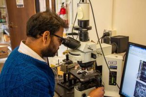
To understand new process they discovered, researchers carefully observed
it using microscopes over course of nearly 3 years.
Untangling that mystery took the better part of 3 years. Agarwal shipped samples of the wires to one of his former graduate students, Pavan Nukala, assistant professor, IISc and member of school’s Centre for Nano Science and Engineering (CeNSE) and one of the paper’s other senior authors.
“Over the past few years we have developed a suite of in situ microscopy tools here at IISc. It was time to put them to test – we had to look very, very carefully to understand this process,” says Nukala. “We learned that multiple properties of In2Se3 – the 2D aspect, the ferroelectricity and the piezoelectricity – all come together to design this ultralow energy pathway for amorphization through shocks.”
Avalanche and earthquake
Ultimately, the researchers found that the process resembles both an avalanche and an earthquake. At first, tiny sections – measured in billionths of a meter – within the In2Se3 wires begin to amorphize as electric current deforms them. Due to the wires’ piezoelectric properties and layered structure, the current nudges portions of these layers into unstable positions, like the subtle shifting of snow at the top of a mountain.
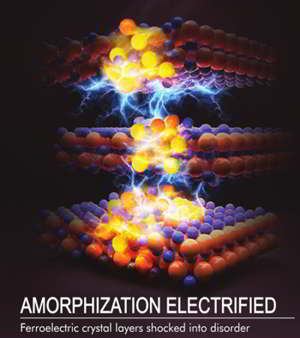
Artist’s impression of electrically driven amorphization in In2Se3, a layered semiconducting ferroelectric material. The middle layer is slipped by the carrier-wind force and the lightning bolts indicate electrical spikes from piezoelectricity induced mechanical shocks, which amorphize the material.
(Credit: Akanksha Jain)
When a critical point is reached, this movement triggers a rapid spread of deformation throughout the wire. The distorted regions collide, producing a sound wave that moves through the material, similar to how seismic waves travel through the earth’s crust during an earthquake.
This sound wave, technically known as an ‘acoustic jerk,’ drives additional deformation, linking numerous small amorphous areas into a single 1 measured in micrometers – 1,000s of times larger than the original areas – just like an avalanche gathering momentum down a mountainside. “It’s just goosebump stuff to see all these phenomena interacting across different length scales at once,” says Shubham Parate, IISc doctoral student and co-first author of the paper.
The collaborative effort to understand the process has created fertile ground for future discoveries.
“This opens up a new field on the structural transformations that can happen in a material when all these properties come together. The potential of these findings for designing low-power memory devices are tremendous,” says Agarwal.
This study was conducted at the University of Pennsylvania School of Engineering and Applied Science, the Indian Institute of Science and the Massachusetts Institute of Technology and supported by the U.S. Office of Naval Research Multidisciplinary University Research Initiatives Program (N00014-17-1-2661), the U.S. National Science Foundation (NSF) Future of Semiconductors competition (#2328743), the U.S. Air Force Office of Scientific Research (FA9550-23-1-0189), the NSF Materials Research Science and Engineering Centers Division of Materials Research (MRSEC/DMR-2309043), and the Anusandhan National Research Foundation Science and Engineering Research Board (CRG/2022/003506) from the Government of India, as well as the facilities at CeNSE and the Advanced Facility for Microscopy and Microanalysis (AFMM), IISc, and the democratized system of usage.
Additional co-authors include Anudeep Tullibilli, IISc; Choah Kwon and Ju Li, MIT; and Andrew C. Meng, Utkarsh Khandelwal, James Horwath, Peter K. Davies and Eric A. Stach, Penn Engineering.
Article: Electrically driven long-range solid-state amorphization in ferroic In2Se3
Nature has published an article written by Gaurav Modi, Department of Materials Science and Engineering, University of Pennsylvania, Philadelphia, PA, USA, Shubham K. Parate, Centre for Nanoscience and Engineering, Indian Institute of Science, Bengaluru, India, Choah Kwon, Andrew C. Meng, Utkarsh Khandelwal, Department of Materials Science and Engineering, University of Pennsylvania, Philadelphia, PA, USA , Anudeep Tullibilli, Centre for Nanoscience and Engineering, Indian Institute of Science, Bengaluru, India, James Horwath, Peter K. Davies, Eric A. Stach, Ju Li, Department of Materials Science and Engineering, Massachusetts Institute of Technology, Cambridge, MA, USA, Pavan Nukala, Centre for Nanoscience and Engineering, Indian Institute of Science, Bengaluru, India, and Ritesh Agarwal, Department of Materials Science and Engineering, University of Pennsylvania, Philadelphia, PA, USA.
Abstract: “Electrically induced amorphization is uncommon and has so far been realized by pulsed electrical current in only a few material systems, which are mostly based on the melt–quench process 1. However, if the melting step can be avoided and solid-state amorphization can be realized electrically, it opens up the possibility for low-power device applications 2,3,4,5. Here we report an energy-efficient, unconventional long-range solid-state amorphization in a new ferroic β″-phase of indium selenide nanowires through the application of a direct-current bias rather than a pulsed electrical stimulus. The complex interplay of the applied electric field perpendicular to the polarization, current flow parallel to the van der Waals layer and piezoelectric stress results in the formation of interlayer sliding defects and coupled disorder induced by in-plane polarization rotation in this layered material. On reaching a critical limit of the electrically induced disorder, the structure becomes frustrated and locally collapses into an amorphous phase6, and this phenomenon is replicated over a much larger microscopic-length scale through acoustic jerks 7,8. Our work uncovers previously unknown multimodal coupling mechanisms of the ferroic order in materials to the externally applied electric field, current and internally generated stress, and can be useful to design new materials and devices for low-power electronic and photonic applications.“


 Subscribe to our free daily newsletter


