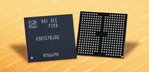
Samsung Start Mass Production V9 TLC V-NAND
Increased data IO/s speeds up to 3.2Gb/s, and cell life extension
This is a Press Release edited by StorageNewsletter.com on July 4, 2024 at 2:02 pmSamsung Electronics recently announced the start of mass production for its 1Tb triple-level cell (TLC) 9th-gen Vertical NAND (V-NAND).

The introduction of V9 TLC V-NAND technology brings something more: a radical enablement of developer applications that suddenly, freed of storage limitations, are empowered to change the world.
V-NAND background
Let’s take a look at how this new-gen of V-NAND alters the status quo. To do so, we’ll evaluate four metrics that define the value of SS V-NAND products as they apply to today’s most significant application areas.
- Bit growth – Essential for AI, autonomous driving, 5G, and cloud services, all of which demand significantly greater storage density than the applications of years past.
- Performance – Faster storage and access mean better options and clarity (and fewer hallucinations) in AI results, quicker response from cloud queries, more rapid and accurate autonomous driving reactions.
- Power consumption – Reducing power draw results in longer battery life, less heat to dissipate, and in the larger scheme of things, a reduced carbon footprint.
- Quality – Each reduction of potential errors, or elimination of a failure path, results in a more reliable and less costly product in terms of TCO.
V9 TLC V-NAND features and benefits
With the metrics clearly established, we can now answer the questions of how, and to what degree, the V9 technology addresses improvements in these metrics.
Bit density. The V9 TLC V-NAND adopted the same 1Tb technology as V8, the industry’s highest bit density, to enable expanded storage space in next-gen servers. This accomplishment required Samsung to develop the industry’s smallest cell size and slimmest mold thickness. It utilizes the company’s unique ‘channel hole etching’ technology, achieved by building an electrically conductive mold stack comprised of hundreds of layers, then vertically piercing cylindrical holes from top to bottom, creating uniform 3D charge trap flash (CTF) cells.
The V9-gen accommodates the greatest number of chip layers in the industry to be drilled simultaneously.
With the notable increase of chip layers, voltage variability across stacks and layers becomes a greater concern. Samsung employs cell voltage penetration techniques to address this issue.
Also contributing to the higher bit density is the firm’s effort to eliminate dummy channel holes, appreciably reducing the size of the memory cells.
Performance. Samsung achieved a top-level V8 I/O speed of 2.4Gb/s using a synchronous DDR interface. The V9-gen introduces the Toggle NAND flash interface (Toggle 5.1), which requires fewer strobe signal transitions to activate a read or write transfer. The result is increased data input/output speeds up to 3.2Gb – 33% faster. To fully take advantage of these blistering speeds, the company supports PCIe 5.0.
Power consumption. From the V8-gen to V9, power consumption improves by 10%. One reason is the Toggle interface mentioned above – with fewer signal transitions, less power is consumed. Another reason is the reduced cell size. The reduction in energy usage makes for key contributions to longer battery life and positive environmental impact.
Quality. Product quality and reliability is enhanced by applying new technology features to V9 V-NAND.
- Cell interference avoidance – With the realization of vastly greater bit density from V8 to V9, interference between and among cells on each layer becomes a greater concern. Company’s technology alleviates this problem through a technique called cell interference avoidance.
- Cell life extension – The number of program/erase (P/E) cycles that can be performed reliably figures strongly into the overall lifetime of the storage device. Higher bit density and the resulting increase in raw storage capacity allow techniques like over-provisioning to lessen the impact of P/E limitations. The firm’s cell life extension technology addresses the flip side of the coin, by addressing the P/E limits themselves.
The value of increased bit density is clearly augmented by the reduction in TCO associated with these features.
Summary
The transition from 8th to 9th-gen TLC V-NAND is more than an evolution. V9 encourages development of applications that were previously either impractical without vast storage capacities and lightning-fast access times, or simply cost-prohibitive.
The fact that V9 techniques will be used in upcoming QLC technology for another leap in density, with PCIe 6.0 for a corresponding leap in speed, will further inspire development with a ‘no limits’ mindset.
Fostered by V9 technology, the paradigm shift has begun. The next-gen of developers, unburdened with the thought that storage has to have capacity limits, will show us the way to world-changing products.


 Subscribe to our free daily newsletter

