Flash Memory Summit: SK hynix Unveils Samples of First 321-Layer 1Tb TLC 4D NAND Flash
And introduced next-gen NAND solutions optimized for such AI demand, including enterprise SSD adopting PCIe Gen5 interface and UFS 4.0.
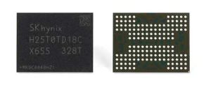
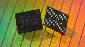
This is a Press Release edited by StorageNewsletter.com on August 9, 2023 at 2:02 pmSK hynix Inc. showcased the sample of the 321-layer 4D NAND, making public the progress on its development of an industry’s first NAND with more than 300 layers.
The company gave a presentation on the progress on the development of its 321-layer 1Tb TLC (*) 4D NAND flash and displayed the samples at FMS) 2023 taking place August 8-10 in Santa Clara, CA.
The firm is the first in the industry to unveil the progress on the development of a NAND with more than 300 layers in detail. The company plans to raise the level of completion of the 321-layer product and start mass production from 1H25.
The company said its technological competitiveness accumulated from the success of the world’s highest 238-layer NAND, already in mass production, paved the way for a smooth progress for the development of the 321-layer product. “With another breakthrough to address stacking limitations, SK hynix will open the era of NAND with more than 300 layers and lead the market.” The 321-layer 1Tb TLC NAND comes with a 59% improvement in productivity, compared with the earlier generation of 238-layer 512Gb, thanks to the technology development that enabled stacking of more cells and larger storage capacity on a single chip, meaning the total capacity that can be produced on a single wafer increased.
Since the introduction of ChatGPT that accelerated the growth of the generative AI market, demand for high-performance and high-capacity memory products that can process more data at a faster pace is growing rapidly.
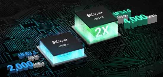
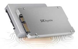
Accordingly, at the FMS, the firm also introduced next-gen NAND solutions optimized for such AI demand, including the enterprise SSD adopting the PCIe Gen5 interface and UFS 4.0.
The company expects these products to achieve leading performance to meet the needs of the customers with a focus on high performance.
The firm announced that it has started development of the next-gen PCIe Gen6 and UFS 5.0 with the improved technology for solution development that it acquired through these products and expressed its commitment to leading the industry trend.
Jungdal Choi, head, NAND development, said during a keynote speech that the company expects the ongoing development of the 321-layer product, the 5th-gen of the 4D NAND, to help the company solidify its technological leadership in the NAND space. “With timely introduction of the high-performance and high-capacity NAND, we will strive to meet the requirements of the AI era and continue to lead innovation.“
(*) TLC: NAND flash products are categorized into single, multi, triple, quadruple and penta level cells depending on the number of information (in bit unit) contained in a single cell. That a cell contains more information means more data can be stored within the same extent of area.


 Subscribe to our free daily newsletter

