YMTC 232-Layer 3D NAND Memory
Despite very challenging context, unexpected technological breakthrough
This is a Press Release edited by StorageNewsletter.com on July 17, 2023 at 2:02 pm![]() By Belinda Dube, technology and cost analyst, Yole SystemPlus, part of Yole Group, and
By Belinda Dube, technology and cost analyst, Yole SystemPlus, part of Yole Group, and
Simone Bertolazzi, PhD, principal technology and market analyst, memory, Yole Intelligence, part of Yole Group.
In 4Q22, YMTC (Yangtze Memory Technologies Corp.) launched its 4th-gen 3D NAND memory, according to the technical report.
Only 3 years after introducing its 2nd-gen chip using a 64-layer package, the Chinese manufacturer has staged a technological coup and broken a record with the release of a new device featuring 232 wordline layers and the highest storage density ever. However, the state of the global memory market and tension between China and USA are a fly in the ointment for YMTC.
At 1st sight, manufacturing 232-layer NAND dies with good yields seems very complex. How did YMTC pull off this feat? This piqued the curiosity of Yole SystemPlus, part of Yole Group, which had already its eye on the Chinese manufacturer’s devices from the beginning. In its latest report – YMTC 232-layer 3D NAND Memory – the analyst company provides insight into the entire manufacturing process and reveals the secrets behind YMTC’s Xtacking architecture. A comparison of the key features of the die with the 64-layer and 128-layer packages is also included.
In its Status of the Memory Industry report, Yole Intelligence asserts that over the past several quarters, the memory markets have faced the most dramatic downturn of the last 15 years. NAND ASPs have fallen 55% since 3Q21 reaching $0.05/GB in early 2023.
The most severe decline started in the final weeks of 2Q22, when a perfect storm of demand-side developments (global conflicts, high inflation, China COVID lockdowns, etc.) crashed into the memory markets.
In addition to the market collapse, YMTC has also been facing strong headwinds due the commercial restrictions set in October 2022 by the U.S. Department of Commerce (DoC); the new rules require U.S. vendors to obtain a license to ship and support 128L-and-above NAND equipment to producers that operate in China.
Despite the very challenging context, YMTC has accomplished significant progress.
Xtacking architecture: YMTC’s NAND memory centerpiece
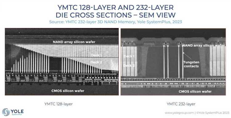
At the very heart of the manufacture of all YMTC’s 3D NAND chips is the Xtacking approach. Known as YMTC’s hallmark, Xtacking involves the use of 2 separate wafers, whereas only one wafer is traditionally employed. It consists of building the NAND dies by joining a CMOS wafer and a NAND array wafer face to face, the 2 wafers being bonded together using metal pads. Both wafers can be manufactured simultaneously, enabling the manufacturer to shorten the production cycle in case of high memory demand.
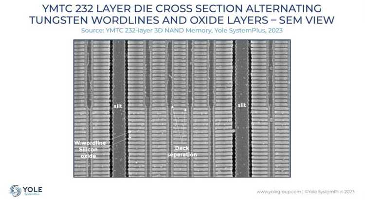
A cross-sectional view of the die shows that 2 decks of alternating tungsten wordlines and SiO layers are formed one after the other. This method was adopted to reduce high aspect ratio etching. If built in one deck, the etch channel aspect ratio would have been 109:1, which would have resulted in very complex trench etching and filling processes and a higher etch defect number.
The strategy is always to find the right balance between yield losses and the cost induced by repeating the etching process. 253 wordlines are observed in the vertical NAND string; 128 layers form deck 1 and 125 form deck 2. Besides the 232 active layers, the remaining ones are divided between dummy and selection layers.
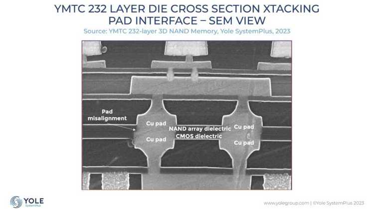
Yole SystemPlus identified the use of a hybrid direct bonding technique to build chemical-free copper-to-copper interconnects that join the wafers together introduced by YMTC in memory manufacturing. Physical interaction between the dielectric material and the copper metal from the 2 wafers forms a strong bond. The bonding interface is further strengthened by plasma treatment of the surfaces and a thermal/annealing process. With this technique, YMTC is able to scale the bonding pad pitch down to 0.8µm. In addition, accurate pad alignment is observed, with a pad mismatch of 22nm representing only 6% of the pad surface.
Key features and comparative analysis of 232-layer 3D NAND memory
As a result of increasingly mastered Xtacking technology, YMTC’s 4th-gen memory chip features faster IO transfer speed and higher storage density. The stacked design combined with a minimized bonding pad and word-line pitches has enabled the company to improve storage density by a factor of 3.5 since the 2nd gen of dies. At 15.47Gb/mm2, the 232-layer NAND chip surpasses Samsung and Micron 176-layer 3D NAND which only reach 10.9Gb/mm² and 10.29Gb/mm², respectively.
The die area has not changed much (an increase of around 5 to 10%) for a capacity that has doubled from one gen to the next (32, 64, and 128GB). As the number of layers has doubled, it was expected that the die thickness would be doubled too. What was true from gen 2 to gen 3 (4.4µm versus 8.6µm) is not the rule for gen 4 (11.9µm). To minimize the total height of the stack, the firm has reduced the wordline pitch by 20% compared to the previous generation.
Facing economic turmoil
Seen as a threat by the major players, it does not yet have a significant market share. Despite its meteoric rise since its creation in 2016 and technological edge, it is still fighting vs. the historical players including Samsung, SK hynix, Micron Technology, Western Digital, and Kioxia and is bearing the brunt of bilateral trade tensions with USA.
About to finalize a major contract with Apple, the Chinese manufacturer was registered on the US Entity List last December (like Huawei 3 years earlier). Furthermore, the memory industry has been facing a severe downturn for a year now, which is expected to continue into the 2H23, according to Yole Intelligence.
How long will the additional funding, provided this year by both private investors and the Chinese government enable YMTC to keep its head above water?
Yole Group at Flash Memory Summit
Once again, Yole Group will be part of the Flash Memory Summit experience as exhibitor and is glad to get the opportunity to meet its customers and business partners, establish new contacts in the industry and help drive your business forward. Simone Bettolazzi, senior technology and market analyst, memory, Mike Howard, VP, DRAM and memory research, and Walt Coon, VP, NAND and memory research, Yole Intelligence, along with Belinda Dude, technology and cost analyst, memory, Yole SystemPlus, will take part of this all-inclusive international memory and storage showcase.
It is the one-stop place to catch up on the latest technologies, see the hottest products, and learn about what’s happening and where the latest trends are heading. FMS is now the largest memory and storage industry show with the most high-level keynoters from leading companies, the largest exhibits, and the most sessions covering everything from applications and architectures through enterprise storage, controllers, and new technologies.


 Subscribe to our free daily newsletter

