Weebit Nano Scaling ReRAM Technology to 28nm With LETI
28nm ReRAM arrays implementing using small and power-efficient switching device, and enabling up to 4x increase in memory density
This is a Press Release edited by StorageNewsletter.com on October 8, 2021 at 1:31 pmWeebit Nano Ltd., with its development partner CEA-Leti, have demonstrated production-level parameters of the company‘s Resistive Random-Access Memory (ReRAM) technology in a 28nm process.
Demonstrating production level parameters of ReRAM technology at 28nm is a step toward productisation of embedded NVM for applications such as AI, autonomous driving, 5G, and advanced IoT processors.
Weebit and CEA-Leti, the French research institute in the field of microelectronics, jointly tested, characterised and measured functional 1Mb ReRAM arrays in a 28nm process technology on 300mm wafers, the largest diameter used in mass production and the standard in advanced nodes.
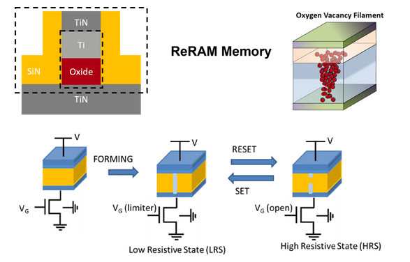
The 28nm ReRAM arrays are implemented using a small and power-efficient switching device, taking advantage of the low power and low voltage capabilities of the 28nm process, and enabling an up to 4x increase in memory density. Testing of the firm’s one-transistor-one-resistor (1T1R) ReRAM arrays, embedded in 28nm Fully Depleted Silicon on Insulator (FDSOI), proved its robustness with good endurance and data retention alongside other production-level quality parameters.
This demonstration of reliability and robustness at 28nm strongly positions the company’s ReRAM technology to be a memory technology in NVM for advanced processes where it is no longer technically or economically feasible to embed flash memory technology.
Olivier Faynot, head, silicon component division, CEA-Leti, said: “The semiconductor industry is constantly moving to smaller geometries for advanced processes. Since embedded flash faces scalability challenges below 40nm, companies today use complex and inefficient solutions when embedding it into their chips. The industry has been crying out for a new technology to succeed flash memory in advanced geometries, and these results show Weebit has a viable solution.“
Commenting on another key development milestone achieved by Coby Hanoch, CEO, Weebit, said: “Weebit, through its close partnership with CEA–Leti, has already demonstrated the significant advantages of its ReRAM technology at larger geometries, and we have now shown that we can successfully scale this technology down to 28nm. Mark Liu, chairman of TSMC, the world’s largest fab, recently called 28nm ‘the sweet spot for our embedded memory applications (*) since the 28nm geometry is widely deployed in a range of applications and is considered the gateway to the most advanced process nodes.
“Given the achievements we have managed in scaling down Weebit’s technology to date, we believe our ReRAM technology can scale to most advanced nodes, enabling Weebit to offer a highly competitive embedded memory solution that replaces flash memory for applications.
“Weebit’s first commercial deal with SkyWater was a major milestone for the Company, providing commercial validation of our innovative technology and enabling us to bring Weebit’s cutting-edge ReRAM technology to volume production at 130nm. With our ReRAM technology now achieving production-level parameters at 28nm, we are expanding the range of potential industries and total addressable market for Weebit’s cutting-edge memory technology.“
(*) Source


 Subscribe to our free daily newsletter


