


3D NAND Market to Grow to $81 Billion in 2025
With 11% CAGR from 2019
This is a Press Release edited by StorageNewsletter.com on November 6, 2020 at 2:13 pmArticle extracted from:
- Equipment and materials for 3D NAND manufacturing 2020, Yole Développement, 2020
- NAND quarterly market monitor, Yole Développement, 3Q20
- YMTC’s 3D NAND flash memory, System Plus Consulting, 2020
3D NAND equipment market: a long-term growth
Highlights:
• 3D NAND has become a mainstream technology because of its excellent scalability that allows increased bit density and lower cost-per-bit via vertical stacking of memory cells.
• Advances in the field of 3D NAND manufacturing are enabled by both equipment and material developments.
• Market figures:
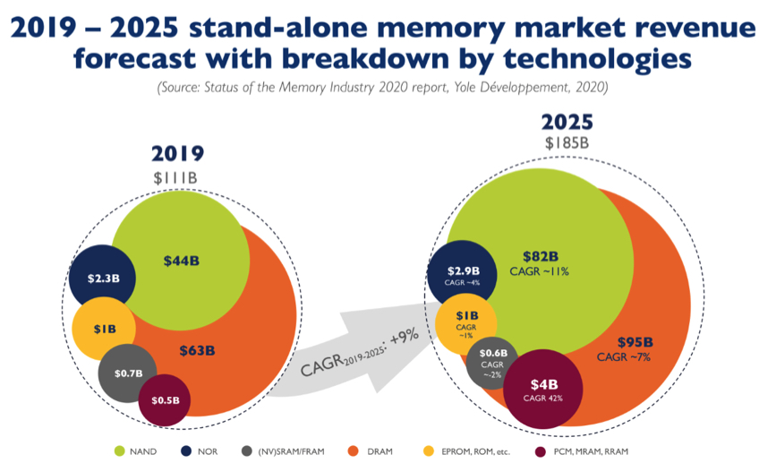
3D NAND market is expected to grow to $81 billion in 2025 with a 11% CAGR between 2019 and 2025. The 3D NAND equipment market including etching, deposition and lithography, will grow to $17.5 billion by 2025, showing a 9% CAGR during the same period.
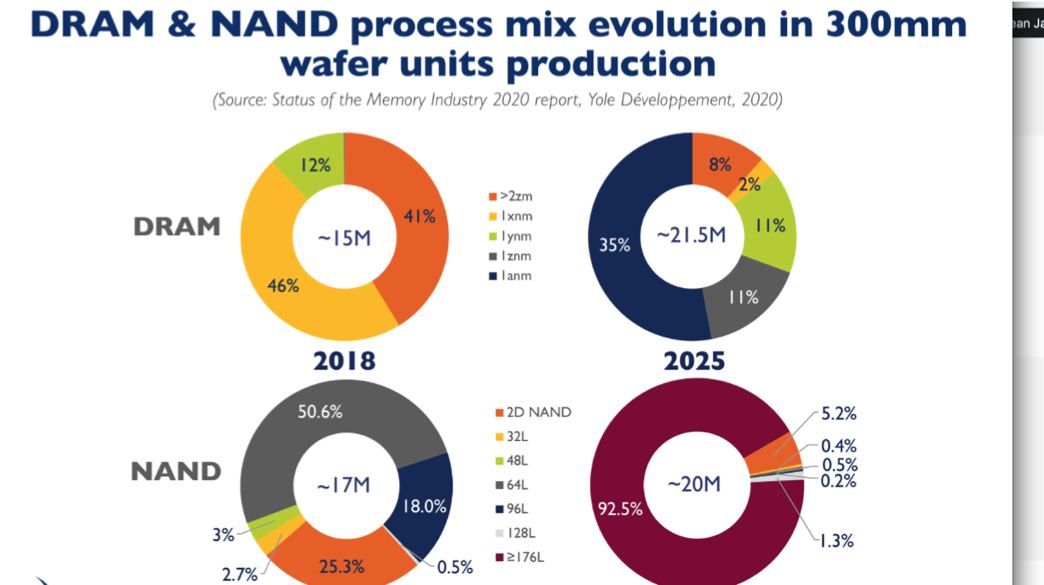
• Technology status: 3D NAND memory manufacturers will adopt different strategies to increase the number of layers and the overall bit density per die.
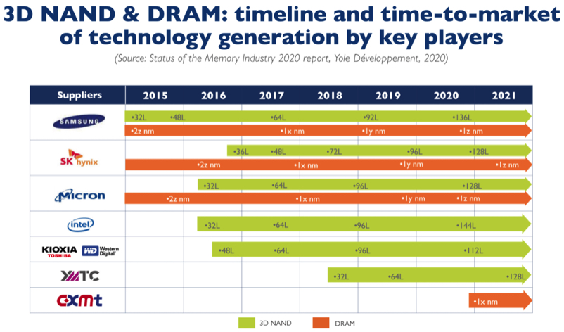
• Competitive landscape: The equipment market is dominated by USA, followed by Japan and Netherland. Four companies, ASML, Applied Materials, Tokyo Electron and Lam Research – hold more than 70% of the overall equipment market. In the 3D NAND business, Samsung is the clear technology leader with fierce competition from WD-Kioxia, followed by SK hynix and Micron-Intel. Leading the NAND memory market in China, YMTC looms on the horizon and threatens to disrupt the status-quo.
Click to enlarge
“The 3D NAND manufacturing equipment market will keep growing, propelled by robust long term NAND-bit demand and ever-increasing manufacturing complexity,” asserts Simone Bertolazzi, PhD, technology and market analyst with the semiconductor and software division, Yole.
The 3D NAND equipment market spanning etching, deposition and lithography equipment is expected to grow from $11 billion in 2019 to $17.5 billion by 2025. This industry will be driven by the etching market segment, with a CAGR around 10%, and deposition, with a CAGR around 9%, between 2019 and 2025.
Four companies are leading this market: Applied Materials, ASML, Tokyo Electron and Lam Research.
For the 3D NAND business, market figures are significant: analysts announce a 9% CAGR between 2019 and 2025 with a growth from $11 to $17.5 billion at the end of the period.
“3D NAND does not require advanced lithography, but it is highly demanding in terms of deposition and etching, as sophisticated HAR (High Aspect Ratio) dry etching tools are needed for processing deep and narrow structures in dielectric stacks,” comments Bertolazzi.
In the NAND Quarterly Market Monitor, 3Q20, analysts affirms that NAND’s competitive landscape remains incredibly dynamic. Samsung is utilizing its massive new Pyeongtaek site and expanding its facilities in Xi’an, China; Kioxia and its partner Western Digital continue to expand their footprint in Japan; Micron and SK Hynix remain competitive despite smaller manufacturing capacities; and Intel has emerged as a stand-alone supplier with capacity in China. In addition, it is also important to notice SK Hynix acquisition of Intel’s NAND business that took place on October 20.
Meanwhile, a new entrant looms on the horizon: China’s YMTC, which threatens to disrupt the status-quo. Indeed, YMTC is the leading NAND memory maker in China.
According to Walt Coon, Yole: “The company is currently shipping 64-layer NAND in low volumes domestically, including SSDs, with 128-layer production under development (shipments expected in 2021). YMTC’s 2020 ramp has been hampered by Covid-19, with delays in equipment deliveries/installations at its Wuhan manufacturing site.“
Belinda Dube, technology and cost analyst, System Plus Consulting, comments: “CMOS periphery and NAND array wafer are manufactured separately. Wafers are connected by copper to copper hybrid bonding. And the bonding technique needs a high level of accuracy and alignment precision to perfectly join the metal layers from different wafers. YMTC’s Xtacking process allows the company to increase its die density.“
YMTC’s memory enters the NAND flash market as a solution to cater for higher I/O speed because of the use of advanced CMOS that can be manufactured on a different wafer from the NAND array. Consequently, this memory provides the combination of high speed and large density characteristics.
In the highly competitive 3D NAND business, there is need for ad hoc tools capable of addressing complex challenges:
• Etching tools must drill deep channel holes from the top of the device to the bottom substrate.
• Deposition tools must produce high-quality defect-free thin films with nm thicknesses.
• Metrology/inspection tools are also becoming essential to monitor the processes and maintain high yields. Ideally, these challenging tasks need to be accomplished in the fastest possible time and lowest cost.
“In this framework, the competition among equipment suppliers to deliver the best solutions is growing fierce,” comments Bertolazzi. “Besides equipment technology development, a great deal of R&D effort has to be focused on finding new material solutions.“
In this context, specific technical strategies are needed for next-gen 3D NAND products.
Three focus areas have been identified by Yole’s memory team:
• String-stacking: whereas all players have already adopted a double-stack approach, Samsung, the industry leader, is the only player to develop the 128-layer gen with a single-string approach and thus enjoys higher margins on NAND than other chip makers. For the following gen, Samsung is expected to adopt double stacking.
• Cell Architecture: all the manufacturers except Intel have adopted the CT (Charge Trap) solution for their 1xx 3D NAND technologies. Intel has recently announced the sale of its 3D NAND business to SK Hynix, and Yole expects they could shift from FG (Floating Gate) to CT as the deal with SK Hynix moves forward. The transfer of the NAND business is expected to be completed by 2025.
• Logic circuit position: besides Micron, with CUA (Circuit-Under-Array), SK Hynix, with 4D-NAND, and YMTC, with Xtacking, all players need to implement specific solutions to minimize the silicon-area consumption of the CMOS logic circuit. Nowadays, all major 3D NAND manufacturers are carrying out R&D activities to explore the use of wafer-to-wafer stacking approaches based on hybrid bonding. Samsung has not yet disclosed an approach to minimize the CMOS logic circuit area and a has strong know∂ci -how in bonding technologies stemming from its CIS (CMOS image sensor) and HBM (High-Bandwidth Memory ) businesses. It could be a potential candidate for the adoption of hybrid bonding for 3D NAND. SK hynix could follow Samsung.


 Subscribe to our free daily newsletter

