Japan’s Floadia Raises ¥1.2 Billion, Total at ¥3.6 Billion
To develop memory technology that could be disruptor in AI edge computing
This is a Press Release edited by StorageNewsletter.com on November 3, 2020 at 2:17 pmFloadia Corporation, headquartered in Kodaira-shi, Tokyo, has raised approximately ¥1.2 billion yen in the series C round of financing.
Using this fund, it will expand its existing embedded memory business and develop a new semiconductor memory technology that can make a breakthrough in AI edge computing with low power consumption.
Teijin Co., Ltd. took the lead position for the series C and undertook a total of ¥530 million together with TEL Venture Capital Inc., a wholly-owned subsidiary of Tokyo Electron, in the first closing. In the second closing, Miyako Capital, Marubeni Ventures Corp., NEC Capital Solutions Ltd., and IDATEN Ventures undertook a total of ¥510 million. Furthermore, Japan Finance Corporation has also provided a loan of ¥180 million.
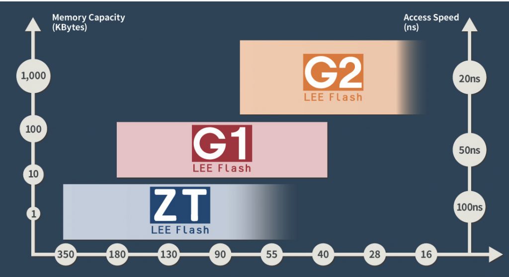
Floadia was founded in 2011 by veteran engineers who left Renesas Electronics. The company licenses its IP, including the manufacturing process and circuit design which enable embedded non-volatile memory production. Its memories are mainly used for micro-computers, power semiconductors, sensors and other semiconductor devices, and reduce power consumption and cost, with auto-grade heat endurance capability. Firm’s non-volatile memory technology is characterized by low power consumption for write/erase operations per memory cell, which is one-millionth of that of competitors (Floadia’s non-volatile memory uses FN tunneling so that power consumption for write/erase operations per memory cell is one-millionth of that of competitors using a hot carrier method.)

Furthermore, the simple manufacturing process enables customers to minimize the development time and reduce the additional manufacturing cost to one-third of that of competitors. Floadia’s memories have been utilized in in-vehicle microcomputers and also adopted in Toshiba microcontrollers. They are also used for smartphone components manufactured by Taiwanese foundries.
These memories can also be embedded without changing other already existing IP designs, making analog/digital integration much easier. As the evolution of 5G smart phones, smart watches, wireless earphones and various battery-powered IoT devices continues, their power consumption, device size and cost will become more essential than ever. In order to further reduce device size and cost, there is an increasing trend to integrate digital circuits and analog circuits on the same chip. Currently, Floadia is working with major foundries to transplant its technology on the 130nm BCD Plus (Bipolar/CMOS/DMOS integrated) platform, and plans mass production from the early part of 2021.
Taking advantage of this funding, Floadia will also accelerate the development of AI edge computing devices that can reduce power consumption.
Currently, AI computing is mainly performed using large-scale data center servers on the cloud side. It is said that AI calculation in the cloud requires enormous power and that there are also data security issues. On the other hand, for AI computing that requires real-time transaction in advanced machines such as autonomous cars and drones, it is essential to perform AI computing on the edge side without connecting to the cloud. By adopting Floadia’s memory technology, it is possible to enhance the power efficiency of AI calculation 100x to 1,000x better.
Floadia had raised about ¥2.4 billion from Innovation Network Corporation of Japan, Ltd. (Japanese government fund), UMC Capital (Taiwanese foundry’s affiliate), Faraday Technology Corp. (Taiwanese ASIC design company), etc.
The total amount of funds raised up to now is approximately ¥3.6 billion.


 Subscribe to our free daily newsletter

