Kioxia Devlops Twin BiCS Flash 3D Semicircular Flash Memory Cell Structure
Candidate to surpass QLC for higher memory density and fewer stacking layers
This is a Press Release edited by StorageNewsletter.com on December 16, 2019 at 2:19 pmKioxia Corporation announced the development of a world’s first [1] 3D semicircular split-gate flash memory cell structure ‘Twin BiCS flash’ using specially designed semicircular Floating Gate (FG) cells.
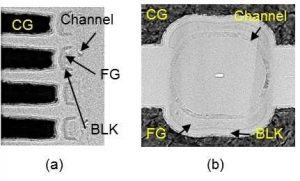
Fabricated semicircular FG cells (a) Cross-sectional view (b) Plane view (figure 1)
Twin BiCS flash achieves superior program slope and a larger program/erase window at a smaller cell size compared to conventional circular Charge Trap (CT) cells. These attributes make this cell design a candidate to surpass QLC for higher memory density and fewer stacking layers.
This technology was announced at the IEEE International Electron Devices Meeting (IEDM) held in San Francisco, CA on December 11t.
3D flash memory technology has achieved high bit density with low cost per bit by increasing the number of cell stacked layers as well as by implementing multilayer stack deposition and high aspect ratio etching. In recent years, as the number of cell layers exceeds 100, managing the trade-offs among etch profile control, size uniformity and productivity is becoming increasingly challenging. To overcome this problem, the company developed a semicircular cell design by splitting the gate electrode in the conventional circular cell to reduce cell size compared to the conventional circular cell, enabling higher-density memory at a lower number of cell layers.
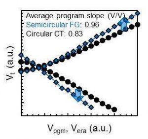
Experimental program/erase characteristics comparing
the semicircular FG cells with the circular CT cells (figure 2)
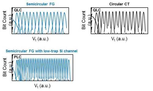
The circular control gate provides a larger program window with relaxed saturation problems when compared with a planar gate because of the curvature effect, where carrier injection through the tunnel dielectric is enhanced while electron leakage to the block (BLK) dielectric is lowered. In this split-gate cell design, the circular control gate is symmetrically divided into two semicircular gates to take advantage of the strong improvement in the program/erase dynamics. As shown in figure 1, the conductive storage layer is employed for high charge trapping efficiency in conjunction with the high-k BLK dielectrics, achieving high coupling ratio to gain program window as well as reduced electron leakage from the FG, thus relieving the saturation issue. The experimental program/erase characteristics in figure 2 reveal that the semicircular FG cells with the high-k-based BLK exhibit gains in the program slope and program/erase window over the larger-sized circular CT cells. The semicircular FG cells, having superior program/erase characteristics, are expected to attain comparably tight QLC Vt distributions at small cell size. Further, integration of low-trap Si channel makes possible more than 4 bits/cell, e.g., Penta-Level Cell (PLC) as shown in figure 3. These results confirm that semicircular FG cells are a viable option to pursue higher bit density.
Simulated Vt distributions after programming using calibrated parameters (figure 3)
Going forward, the company’s R&D efforts aimed at innovation in flash memory will include continuing Twin BiCS flash development and seeking its practical applications.
At IEDM 2019, the firm also announced six other papers highlighting the company’s intensive R&D activities in the area of flash memory.
[1] Source: Kioxia Corporation, as of December 12, 2019


 Subscribe to our free daily newsletter

