Toshiba Shipping Samples of 64-Layer, 512Gb 3D Flash Memory
1TB product with 16-die stacked architecture in single package
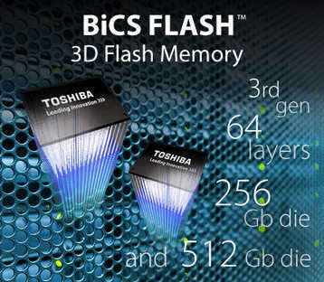
This is a Press Release edited by StorageNewsletter.com on February 27, 2017 at 2:38 pmToshiba Corporation has unveiled the latest addition in its industry line-up of BiCS Flash three-dimensional flash memory with a stacked cell structure (1), a 64-layer device that achieves a 512Gb (64GB) capacity with 3-bit-per-cell (TLC) technology.

This device will be used in applications that include enterprise and consumer SSD. Sample shipments of the chip started this month, and mass production is scheduled for the second half of this calendar year.
The company continues to refine BiCS flash, and the next milestone on its development roadmap is the industry’s largest capacity (2), a 1TB product with a 16-die stacked architecture in a single package. Plans call for the start of sample shipments in April 2017.
For the 512Gb device, the firm deployed 64-layer stacking process to realize a 65% larger capacity per unit chip size than the 48-layer 256Gb (32GB) device, and has increased memory capacity per silicon wafer, reducing the cost per bit.
Company’s memory business already mass produces 64-layer 256Gb (32GB) devices and will expand BiCS flash production. It will advance 3D technology to realize increased densities and finer processes in order to meet diversifying market needs.
Note:
[1] A structure stacking flash memory cells vertically on a silicon substrate to realize density improvements over planar NAND flash memory, where cells are formed on the silicon substrate.
[2] As of February 22, 2017. Company’s survey.


 Subscribe to our free daily newsletter


